Researchers at the University of Utah have created one of the most minuscule plasma transistors that can resist soaring temperatures and ionizing radiation that could be seen in a nuclear reactor. The engineers envision that such transistors would:
1) Facilitate taking and collecting X-rays in war zones by high-end cellular phones
2) Integrated within equipments to gauge air quality in the actual time
3) Plasma based bot could be sent into the nuclear reactor for certain assignments
Like beavers, the transistors perform the most important work in the field of electronics. Generally, these are created as a single entity but work in unison in form of coupled pieces on a particular computer chip. They act like a gatekeeper – where silicon is used as a valve of the gate – and check the flow of the electricity within devices.
Silicon based transistors
Nuclear reactors normally operate above 550 degrees Fahrenheit this creates a major huddle with transistors that are based on silicon, since the latter fails to synchronize at that temperature. On the other hand plasma-based transistors functions at more than 300 volts that calls for high-voltage sources.
Transistors based on plasma that employs ionized gas for conducting electricity are used in light sources, medical equipments and other sources that operate in the presence sunlight. These tools are highly miniscule, somewhere around width of five human hairs.
Plasma based transistors
The newly evolved transistors based on plasma are around 1 micron to 6 microns, which means, 500 times smaller functioning at one-sixth of the voltage relatively. These can easily work at temperatures around 1,450 degrees Fahrenheit, which is more than double at which silicon operates. Hence, they are the perfect candidate for nuclear reactors.
These ionized based transistors have a huge potential in initiating a completely new wave of electronic devices, asserted Tabib-Azar, the lead researcher.
Utah Microplasma Transistor: Research & Applications
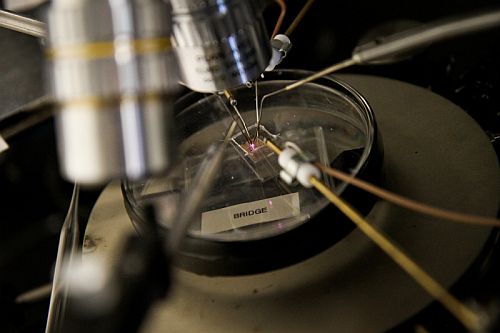
Traditionally two conjoined active layers over one another forms a transistor. Electric current passes through one layer while the other sheet controls the flow. However, for the study, researchers set down sheets of metal alloy to form a gate or to control the flow of electricity on a four- inch glass wafer. Then a sheet of silicon was placed on top of the metal alloy.
It is the air gap in the new transistor that transmits ions and electrons from plasma upon applying the voltage, a phenomena which is not seen in conventional transistors.
This air gap is created by etching away the silicon film in the transistor. A chemically reactive gas is employed for the scrapping. Once the silicon is removed, the 2 microns wide and 10 microns long spaces were formed which was made to occupy by helium. Hence plasma based connections were created that is very much different from the conventional metal based connections. Researchers assert that the new connections will work only when they are powered up, in absence of the power source, it will disappear, which makes them appropriate for military applications.
Its smaller dimension would make it fitting element for transistors based smartphones, where it might be used for taking and carrying x-rays images of injured soldier in battlefield.
In the coming few years, these transistors based devices might also find its place in identifying aerosol pollutants, thus helping researchers in monitoring and constructing air quality map with precision.
Source: Phys.org